- 您现在的位置:买卖IC网 > Sheet目录3871 > PIC18F4682T-I/ML (Microchip Technology)IC PIC MCU FLASH 40KX16 44QFN
2011 Microchip Technology Inc.
DS39931D-page 109
PIC18F46J50 FAMILY
7.5
Writing to Flash Program Memory
The programming block is 32 words or 64 bytes.
Programming one word or 2 bytes at a time is also
supported.
Table writes are used internally to load the holding reg-
isters needed to program the Flash memory. There are
64 holding registers used by the table writes for
programming.
Since the Table Latch (TABLAT) is only a single byte, the
TBLWT
instruction may need to be executed 64 times for
each programming operation (if WPROG = 0). All of the
table write operations will essentially be short writes
because only the holding registers are written. At the
end of updating the 64 holding registers, the EECON1
register must be written to in order to start the
programming operation with a long write.
The long write is necessary for programming the
internal Flash. Instruction execution is halted while in a
long write cycle. The long write will be terminated by
the internal programming timer.
The on-chip timer controls the write time. The
write/erase voltages are generated by an on-chip
charge pump, rated to operate over the voltage range
of the device.
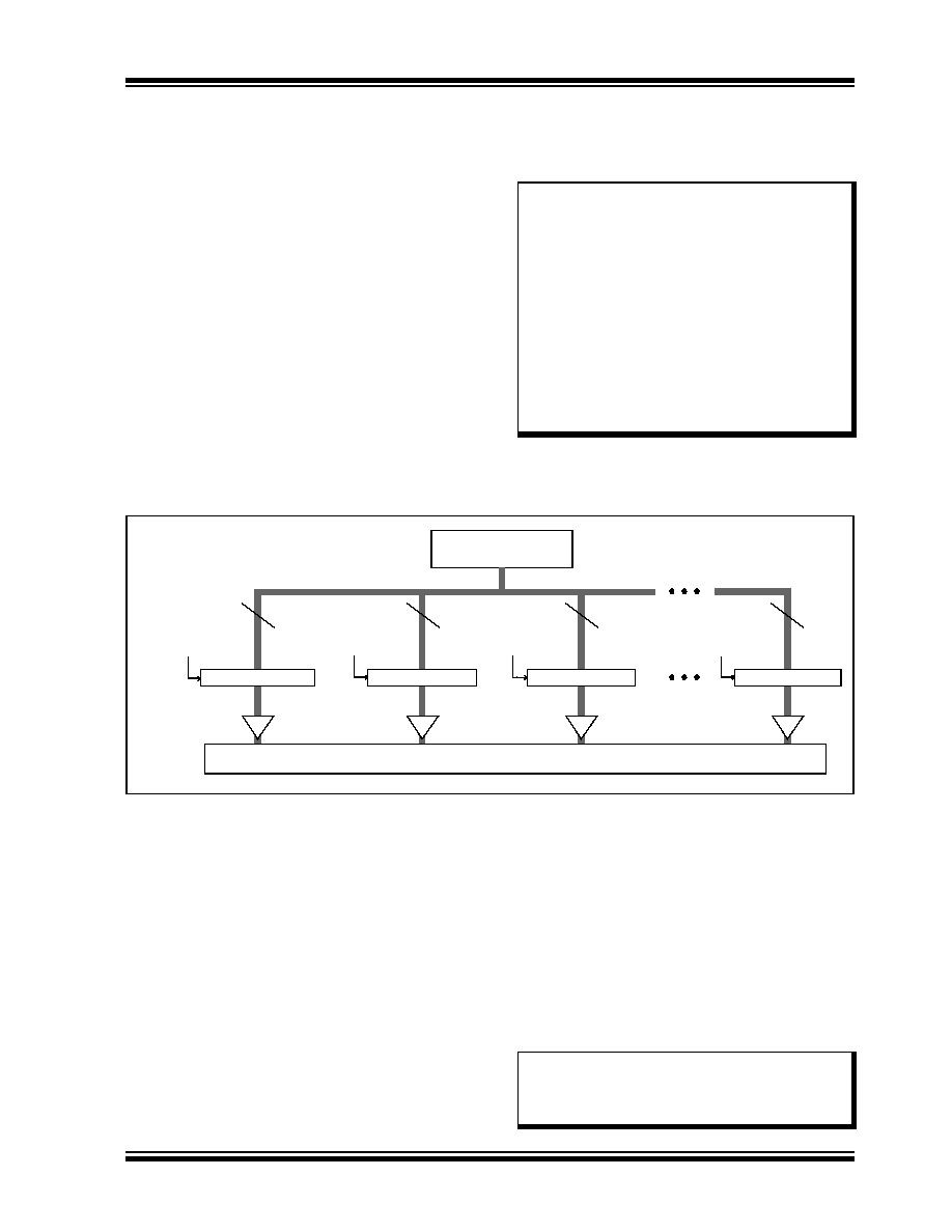
FIGURE 7-5:
TABLE WRITES TO FLASH PROGRAM MEMORY
7.5.1
FLASH PROGRAM MEMORY WRITE
SEQUENCE
The sequence of events for programming an internal
program memory location should be:
1.
Read 1024 bytes into RAM.
2.
Update data values in RAM as necessary.
3.
Load the Table Pointer register with the address
being erased.
4.
Execute the erase procedure.
5.
Load the Table Pointer register with the address
of the first byte being written, minus 1.
6.
Write the 64 bytes into the holding registers with
auto-increment.
7.
Set the WREN bit (EECON1<2>) to enable byte
writes.
8.
Disable interrupts.
9.
Write 0x55 to EECON2.
10. Write 0xAA to EECON2.
11. Set the WR bit. This will begin the write cycle.
12. The CPU will stall for the duration of the write for
13. Re-enable interrupts.
14. Repeat Steps 6 through 13 until all 1024 bytes
are written to program memory.
15. Verify the memory (table read).
An example of the required code is provided in
Example 7-3 on the following page.
Note 1:
Unlike previous PIC devices, devices of
the PIC18F46J50 family do not reset the
holding registers after a write occurs. The
holding registers must be cleared or
overwritten before a
programming
sequence.
2:
To maintain the endurance of the pro-
gram memory cells, each Flash byte
should not be programmed more than
once between erase operations. Before
attempting to modify the contents of the
target cell a second time, an erase of the
target page, or a bulk erase of the entire
memory, must be performed.
TABLAT
TBLPTR = xxxx3F
TBLPTR = xxxxx1
TBLPTR = xxxxx0
Write Register
TBLPTR = xxxxx2
Program Memory
Holding Register
8
Note:
Before setting the WR bit, the Table
Pointer address needs to be within the
intended address range of the 64 bytes in
the holding register.
发布紧急采购,3分钟左右您将得到回复。
相关PDF资料
PIC24HJ128GP306T-I/PT
IC PIC MCU FLASH 128KB 64TQFP
PIC24FJ96GA008T-I/PT
IC PIC MCU FLASH 96KB 80TQFP
PIC24FJ64GA010T-I/PT
IC PIC MCU FLASH 64KB 100TQFP
PIC24FJ64GA008T-I/PT
IC PIC MCU FLASH 64KB 80TQFP
PIC18LF4450T-I/PT
IC PIC MCU FLASH 8KX16 44TQFP
PIC18LF2450T-I/ML
IC PIC MCU FLASH 8KX16 28QFN
PIC16F1937-I/ML
IC PIC MCU FLASH 512KX14 44-QFN
PIC18F25K20-E/ML
IC PIC MCU FLASH 16KX16 28-QFN
相关代理商/技术参数
PIC18F4682T-I/PT
功能描述:8位微控制器 -MCU 80KB FL 3328bytes RAM 36I/O RoHS:否 制造商:Silicon Labs 核心:8051 处理器系列:C8051F39x 数据总线宽度:8 bit 最大时钟频率:50 MHz 程序存储器大小:16 KB 数据 RAM 大小:1 KB 片上 ADC:Yes 工作电源电压:1.8 V to 3.6 V 工作温度范围:- 40 C to + 105 C 封装 / 箱体:QFN-20 安装风格:SMD/SMT
PIC18F4685-E/ML
功能描述:8位微控制器 -MCU 96KB 3328 RAM w/ECAN RoHS:否 制造商:Silicon Labs 核心:8051 处理器系列:C8051F39x 数据总线宽度:8 bit 最大时钟频率:50 MHz 程序存储器大小:16 KB 数据 RAM 大小:1 KB 片上 ADC:Yes 工作电源电压:1.8 V to 3.6 V 工作温度范围:- 40 C to + 105 C 封装 / 箱体:QFN-20 安装风格:SMD/SMT
PIC18F4685-E/P
功能描述:8位微控制器 -MCU 96KB 3328 RAM w/ECAN RoHS:否 制造商:Silicon Labs 核心:8051 处理器系列:C8051F39x 数据总线宽度:8 bit 最大时钟频率:50 MHz 程序存储器大小:16 KB 数据 RAM 大小:1 KB 片上 ADC:Yes 工作电源电压:1.8 V to 3.6 V 工作温度范围:- 40 C to + 105 C 封装 / 箱体:QFN-20 安装风格:SMD/SMT
PIC18F4685-E/PT
功能描述:8位微控制器 -MCU 96KB FL 3328bytes RAM 36I/O RoHS:否 制造商:Silicon Labs 核心:8051 处理器系列:C8051F39x 数据总线宽度:8 bit 最大时钟频率:50 MHz 程序存储器大小:16 KB 数据 RAM 大小:1 KB 片上 ADC:Yes 工作电源电压:1.8 V to 3.6 V 工作温度范围:- 40 C to + 105 C 封装 / 箱体:QFN-20 安装风格:SMD/SMT
PIC18F4685-I/ML
功能描述:8位微控制器 -MCU 96KB 3328 RAM w/ECAN RoHS:否 制造商:Silicon Labs 核心:8051 处理器系列:C8051F39x 数据总线宽度:8 bit 最大时钟频率:50 MHz 程序存储器大小:16 KB 数据 RAM 大小:1 KB 片上 ADC:Yes 工作电源电压:1.8 V to 3.6 V 工作温度范围:- 40 C to + 105 C 封装 / 箱体:QFN-20 安装风格:SMD/SMT
PIC18F4685-I/ML
制造商:Microchip Technology Inc 功能描述:IC 8BIT MCU PIC18F 40MHZ QFN-44 制造商:Microchip Technology Inc 功能描述:IC, 8BIT MCU, PIC18F, 40MHZ, QFN-44
PIC18F4685-I/P
功能描述:8位微控制器 -MCU 96KB 3328 RAM w/ECAN RoHS:否 制造商:Silicon Labs 核心:8051 处理器系列:C8051F39x 数据总线宽度:8 bit 最大时钟频率:50 MHz 程序存储器大小:16 KB 数据 RAM 大小:1 KB 片上 ADC:Yes 工作电源电压:1.8 V to 3.6 V 工作温度范围:- 40 C to + 105 C 封装 / 箱体:QFN-20 安装风格:SMD/SMT
PIC18F4685-I/P
制造商:Microchip Technology Inc 功能描述:8-Bit Microcontroller IC